SEMICON Korea 2026
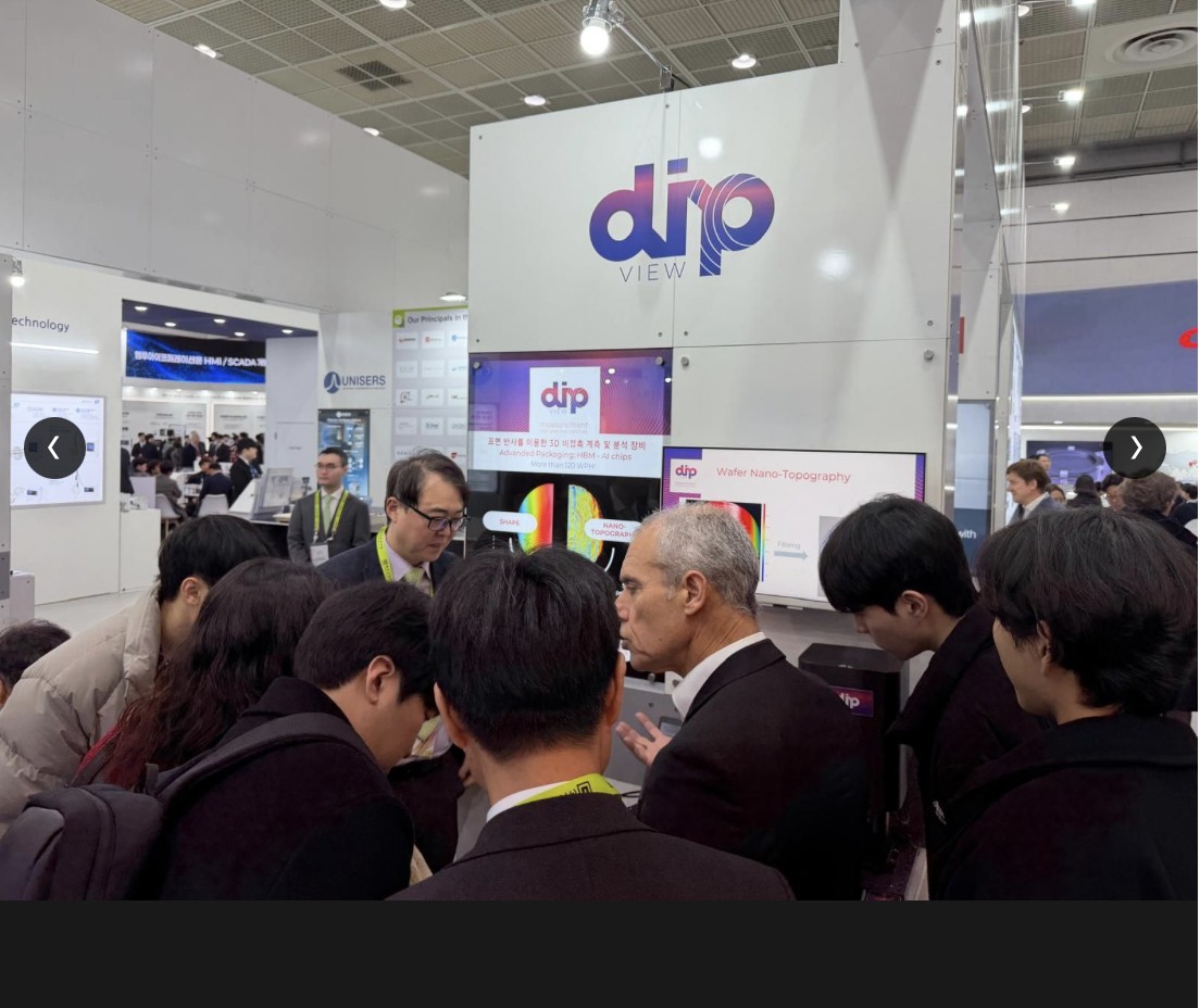
Great success at SEMICON Korea, where DIP-View introduced its Advanced Packaging Metrology leveraging High Resolution Deflectometry. Thanks to everyone who visited our booth, and to our local partner Woowon Technology.
VISION 300 — one platform, five integrated measurement domains, one seamless workflow. Wafer geometry, nano-topography, film thickness, bonding metrology and surface inspection, intrinsically co-registered.
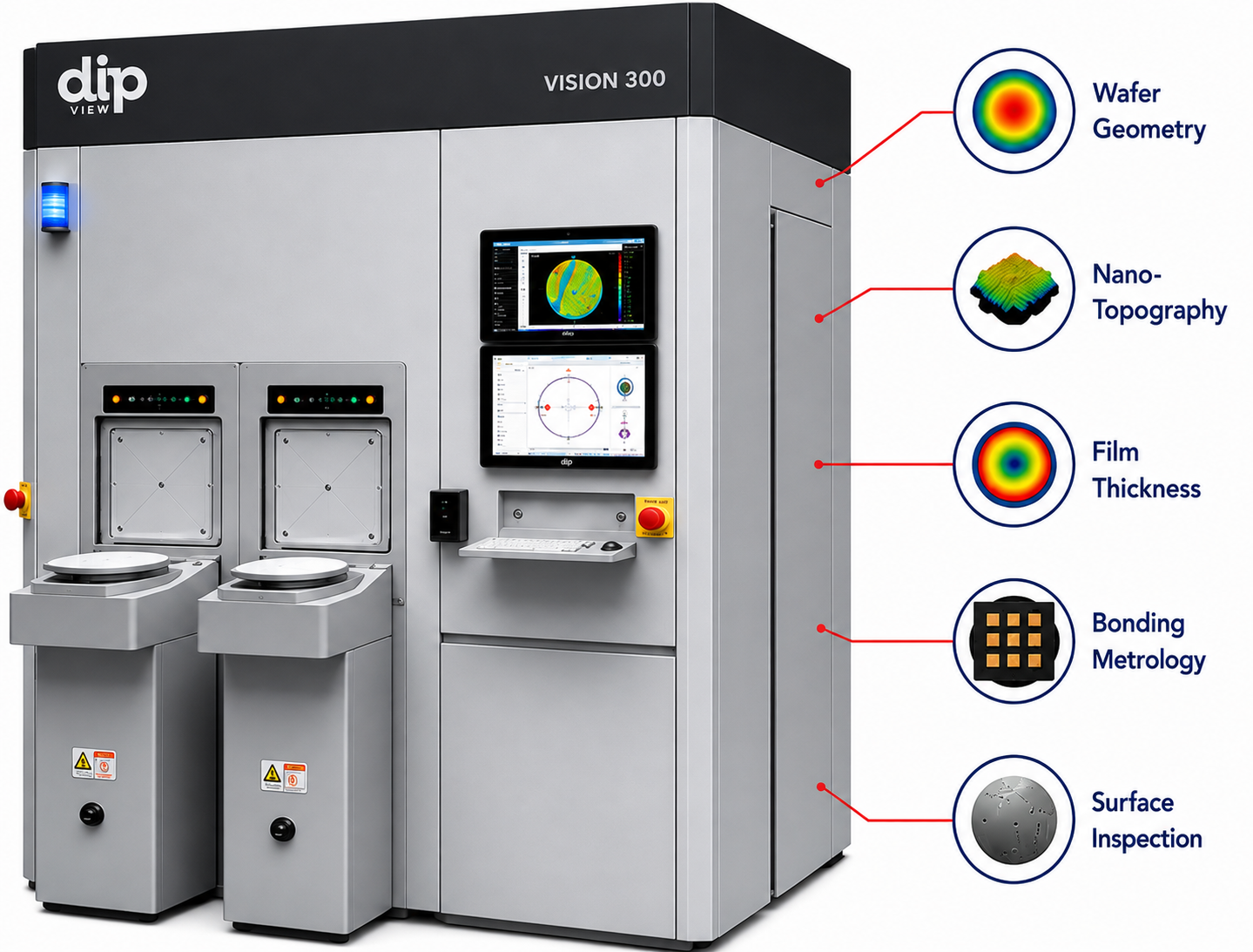
DIP-View is a pioneer in High Resolution Deflectometry, allowing us to reach nanometer accuracy across the full 300 mm wafer surface. This powerful technology is at the heart of VISION 300, our integrated wafer metrology platform.
One platform, five measurement domains, one workflow — built exclusively for semiconductor manufacturers moving to D2W and W2W advanced packaging.
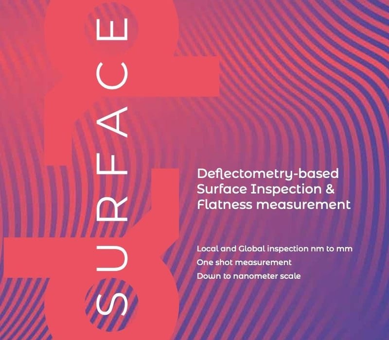
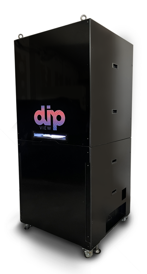
A closer look at the VISION 300 hardware — engineered and assembled for nanometer-scale wafer metrology.

Serial entrepreneur in high tech industries — Leading International Business Development.

PhD in Physics and microelectronics, Senior Research fellow at LAAS, with a successful track record in Research to Industry technology transfers.

Innovative research optical engineer, expert in optical design and instrumentation software.
A unique integrated platform combining wafer geometry, nano-topography, film thickness, bonding metrology and surface inspection within a seamless measurement workflow.
All measurements are acquired on the same platform, intrinsically co-registered and analyzed within a unified software environment. By eliminating data correlation across multiple tools, VISION 300 accelerates process development, improves process control and enables faster, more confident manufacturing decisions.
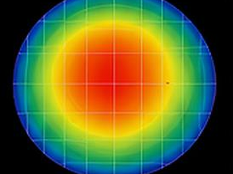
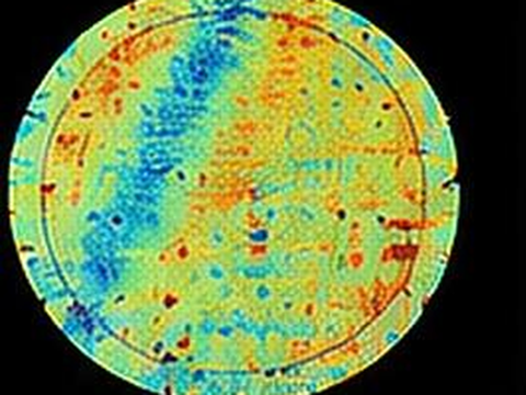
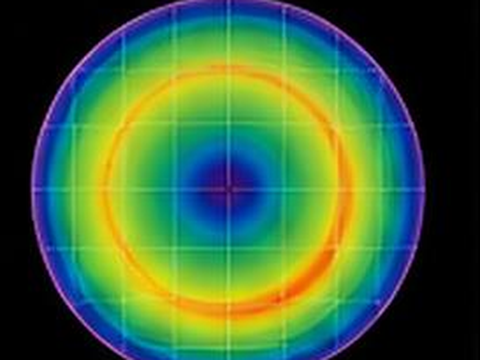
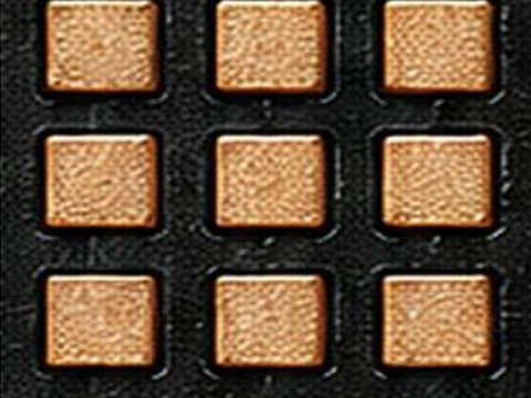
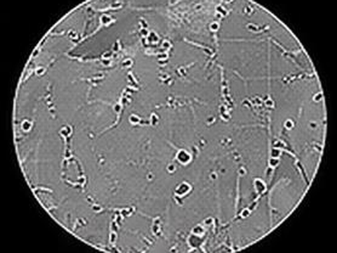
Helping manufacturers improve yield through better process understanding.
VISION 300 enables semiconductor manufacturers to detect, understand and correlate the process signatures that impact yield, reliability and manufacturing efficiency across advanced semiconductor applications.
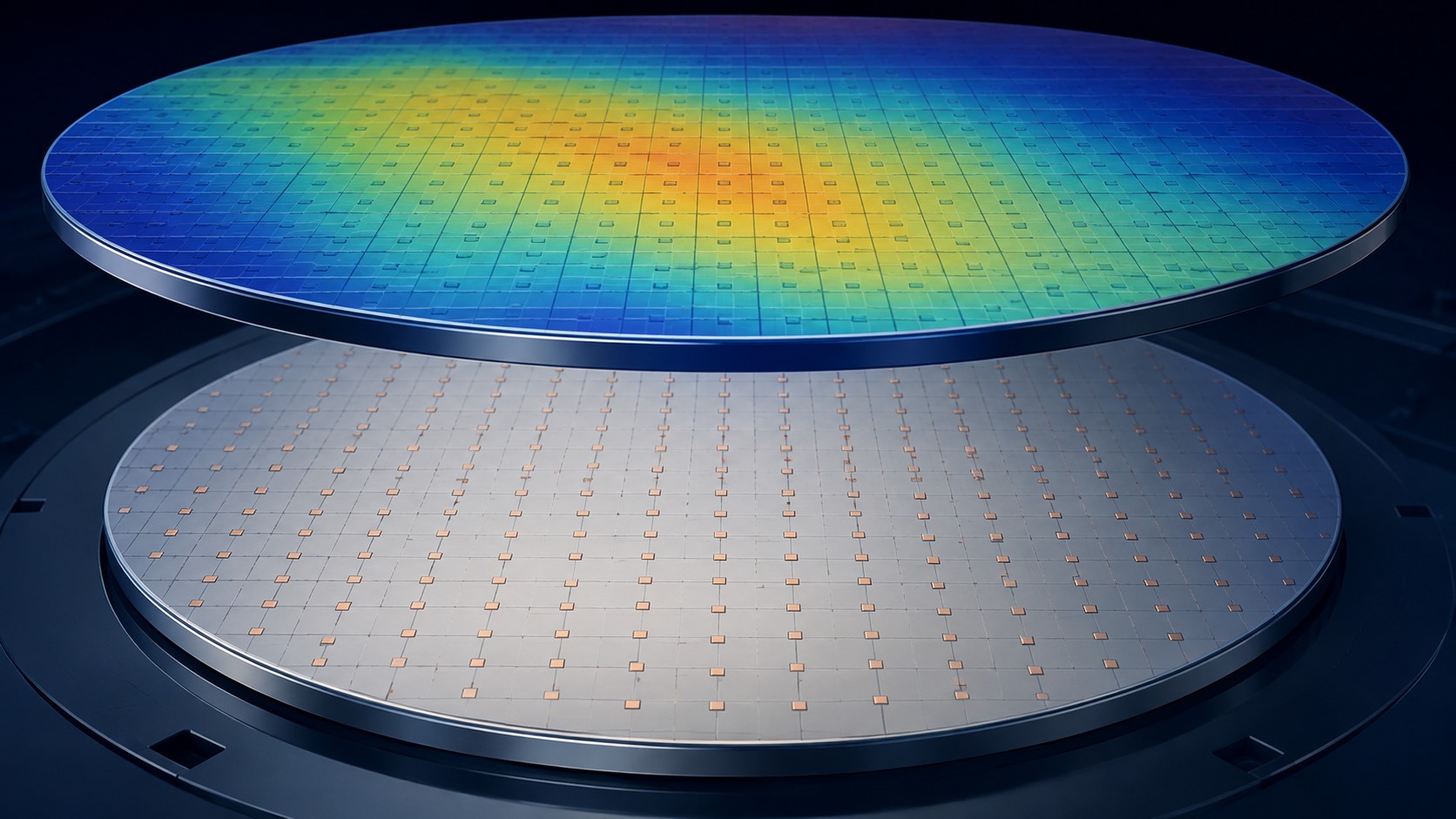
Improve bonding readiness before wafers ever touch.
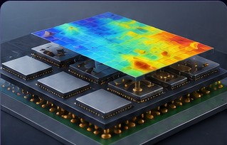
Control deformation across increasingly complex packages.
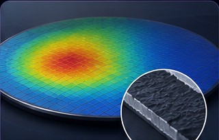
Detect process variations before they impact downstream manufacturing.
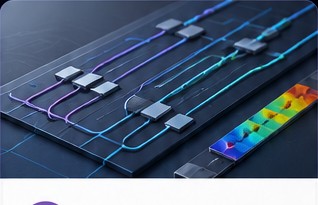
Improve process uniformity for next-generation photonic devices.
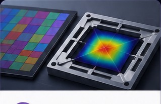
Characterize functional surfaces across large-area devices.
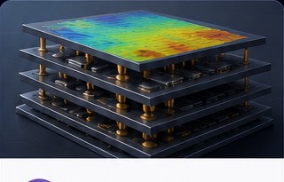
Monitor deformation through successive integration steps.









Great success at SEMICON Korea, where DIP-View introduced its Advanced Packaging Metrology leveraging High Resolution Deflectometry. Thanks to everyone who visited our booth, and to our local partner Woowon Technology.
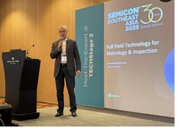
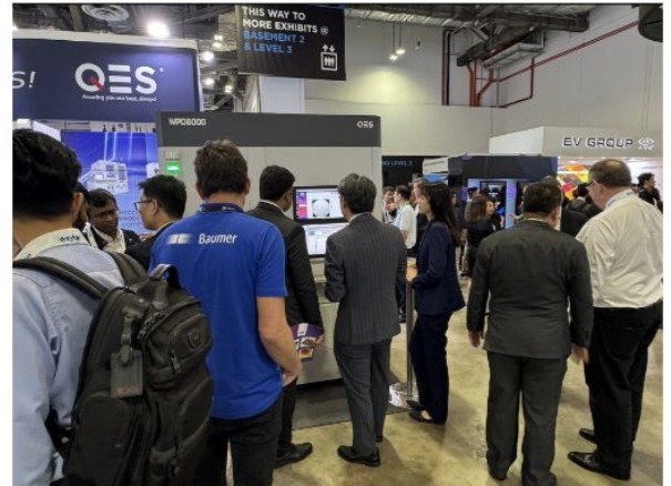
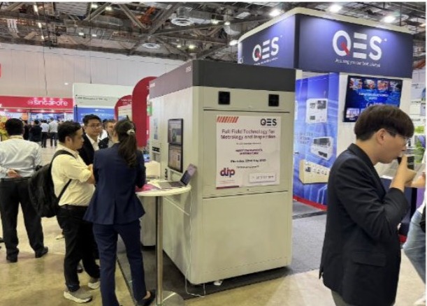
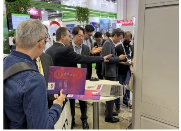
Proud to present our VISION 300 product at SEMICON SEA, featuring full automation with QES wafer robotics — merging Advanced Wafer Metrology and Defect Macro-Inspection into a single solution.

From Toulouse to Taiwan! DIP-View is taking its Asian expansion to the next level after a successful debut at SEMICON 2024 — exciting discussions on advanced packaging, warpage and nano-topography metrology.
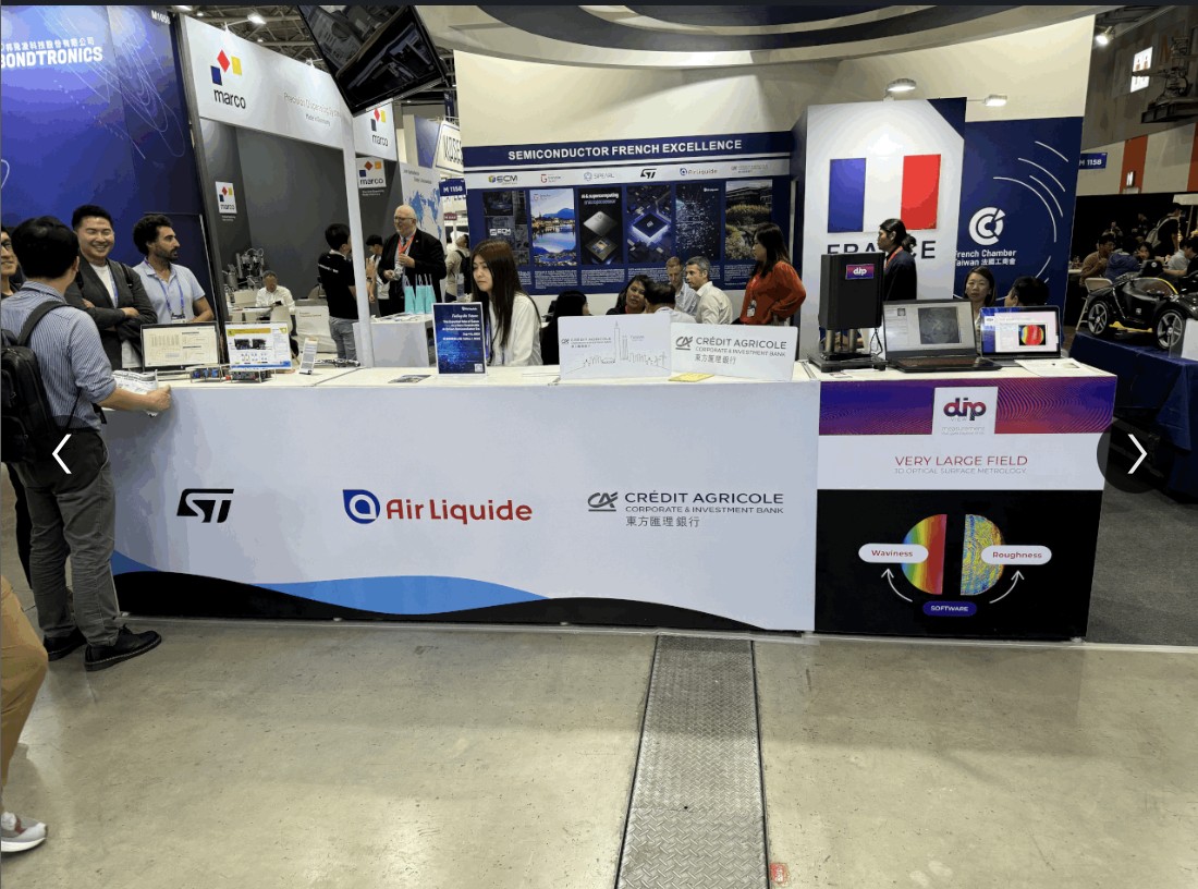
DIP-View hosted Thomas Courbe from the French Economy Ministry (DGE) at SEMICON Taiwan's French Pavilion, with collaborations underway with ITRI and CEA.
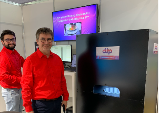
DIP-View presented its latest technologies for 3D wafer inspection: a full static measurement of Bow, Warp, TTv, LTv with dual wafer side capabilities up to 300 mm. From mm to nm in one single shot!

BPI France has recognised DIP-View's innovative technology for the 3D surface inspection market. DIP-View is now listed as a French DEEPTECH company.
DIP-View has joined SEMI to contribute actively to the development of metrology technologies in the semiconductor market, and AENEAS, the industrial association supporting funding access for micro and nanoelectronics R&D&I participants.